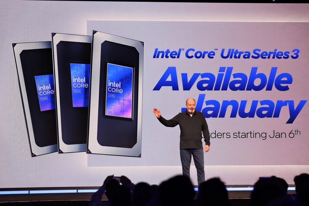
Intel is not just re-launching a product lineup; it is reviving an entire industrial cycle. At the CES 2026, the company unveiled the Core Ultra Series 3, marking the release of the first fully integrated client PC platform manufactured using its Intel 18A process. This launch is less about showcasing raw power and more about demonstrating maturity, featuring a complete System-on-Chip (SoC) designed to validate every component—CPU, GPU, neural processing unit (NPU), memory, and I/O—under the practical constraints of a professional laptop.
For several generations, Intel has navigated hybrid architectures, fragmented processes, and shifting timelines. Alder Lake and Raptor Lake were built on the Intel 7 process, while Meteor Lake introduced a tiled architecture but relied on TSMC for several blocks due to its internal Intel 4 process lacking readiness. These ongoing compromises have weakened the coherence between design and manufacturing, leading to noticeable impacts on consumption, effective density, and thermal stability.
Core Ultra Series 3 aims to reverse this trend. For the first time in over a decade, Intel has produced a complete, client-side SoC entirely on a single node without depending on an external foundry. The Intel 18A node is not merely an incremental upgrade; it leverages a new generation of RibbonFET transistors with a surrounding gate design and PowerVia back-silicon power delivery, which reconfigures the physical structure of the component.
### A CPU Engineered for Stability Under Load
The CPU architecture features a hybrid arrangement, blending performance and efficiency cores akin to previous generations. However, Intel has fine-tuned the number and frequencies of these cores to fit the thermal envelope of ultra-thin chassis. The goal is not to achieve bursts of peak performance but to ensure stability under sustained loads with predictable behavior, avoiding overheating and software throttling.
Intel estimates that the transition from Intel 3 to 18A yields roughly a 15% performance-per-watt increase at constant frequencies. This improvement arises from reduced leakage currents courtesy of RibbonFET and stabilized power supply through PowerVia, which diminishes voltage droop and resistive losses in the upper layers of the chip.
### An Integrated GPU Designed for Continuity
The integrated graphics unit is based on the Arc Xe architecture but is configured with minimized compute units to avoid over-provisioning. This decision aligns with the intended use cases: multi-monitor setups, video encoding/decoding, and 2D/3D visualization, while consciously avoiding gaming or intensive creative workloads. It’s a GPU designed for users who consistently utilize their graphics card but do not require extreme performance.
The compact die enabled by 18A density facilitates direct integration into the SoC, yielding valuable space for thermal dissipation. Intel aims to achieve measurable improvements in graphical performance consistency over extended sessions, especially by mitigating frequency drops caused by temperature spikes.
### A Locally Optimized AI Engine for Efficiency
The AI accelerator features a dedicated Neural Processing Unit (NPU), an architecture developed by Intel for on-device processing. This NPU is optimized for inference of compact, quantized models and operates independently of the CPU and GPU. It targets applications such as context-aware assistants, local voice transcription, low-latency event detection, and dynamic application optimization.
This unit is not intended for executing massive models. It’s designed for consistent workloads with low power consumption, yielding up to 50 TOPS aggregated across the SoC, depending on configuration, while emphasizing energy efficiency to extend battery life rather than raw power.
### Memory and I/O Designed for Overall Coherence
The integrated memory controller manages LPDDR5X with optimized timings for swift access in multitasking scenarios. The tight integration within the SoC reduces global latency, directly enhancing performance in office tasks, multitasking browsing, or executing local AI agents.
The I/O blocks include PCIe Gen 5 and USB4 links, integrated into the SoC logic to simplify routing and reduce losses. This approach allows Intel to offer a streamlined, firmware-controlled platform that maintains stable performance even under multiple-component interactions—a critical aspect for professional mobile users.
### Intel 18A: Density and Efficiency
The RibbonFET transistors provide better control over the channel, allowing for lower operating voltages without sacrificing frequency. PowerVia eliminates overhead power networks above the silicon, reducing interconnection congestion and freeing up space for denser structures. Intel claims a 30% improvement in logic density compared to Intel 3.
Beyond the figures, what truly changes is the ability to integrate what were once distinct blocks into a single SoC without compromising thermal efficiency or performance consistency. The Core Ultra Series 3 exemplifies this balance between density, battery life, and stability, made possible by a truly internally controlled node.
With this platform, Intel is not just vying for market share in the professional laptop segment. It aims to validate, piece by piece, a fully internal design and production chain. The Core Ultra Series 3 represents the first commercially available product to emerge in volume from the 18A process. The company seeks to demonstrate that it can independently deliver a complete, competitive, and stable SoC once again.
In a landscape where AMD depends on TSMC for its mobile Ryzen chips and Qualcomm promotes its Arm-based Copilot chips, Intel is positioning itself as a sovereign x86 alternative grounded in its own fabrication facilities. This promise of reliability, supply stability, and energy control is what the Core Ultra Series 3 is poised to embody, far beyond its raw specifications.