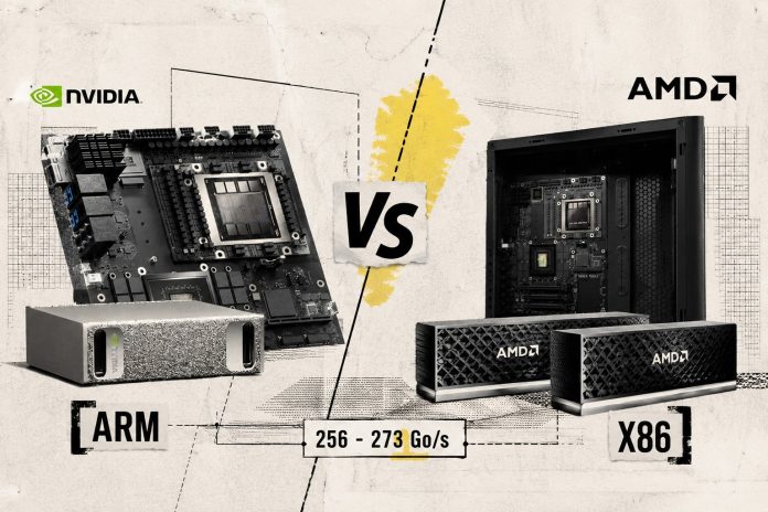
Local inference workstations with unified memory are emerging as a standalone product line. Nvidia and AMD are adopting two distinct architectures for this purpose: an Arm-based processor paired with a dedicated GPU on one side and an all-in-one x86 processor on the other, both boasting similar memory capabilities. However, they encounter the same physical limitation — a bandwidth of 256 to 273 GB/s restricts generation speed. Differentiation lies in their intended uses, ranging from data center prototyping to individual workstations designed for everyday tasks.
Local inference has redefined the role of video memory, which previously catered primarily to gaming and graphic computation, where power triumphed over capacity. It now dictates the workloads a workstation can handle. A GeForce RTX 5090 maxes out at 32 GB of GDDR7, making it impossible to load a model of 70 billion parameters without segmenting it between the GPU and the main memory, necessitating PCIe transfers at each layer. Practitioners resort to clever tricks and logical partitioning tools to stay within this limit, often at the cost of degrading response times.
Both Nvidia and AMD have sidestepped this hurdle by implementing a unified LPDDR5X memory that is shared between the processor and the GPU over a 256-bit bus. This approach eliminates PCIe transfers and expands the addressable capacity well beyond that of a dedicated graphics card, although it does come with significantly lower bandwidth, approximately one-third that of GDDR7. The paths they took to reach these architectures reflect two different industrial trajectories and product cultures.
Two Lineages: Data Center Arrays and Console APUs
The DGX Spark is a direct descendant of Nvidia’s learning arrays. The DGX series initially served as training cabinets for data centers, starting from the original DGX-1 to the GB200 NVL72 cabinets, alongside a desktop variant that retains the architectural foundation of these arrays — a Grace processor combined with a Blackwell GPU. Grace is Nvidia’s proprietary Arm processor line developed after its failed acquisition of Arm, and it was with the first Grace Hopper assembly that NVLink-C2C was introduced, allowing the GPU to access CPU memory without copying.
Arm presents the DGX Spark as a continuation of Grace Hopper and Grace Blackwell, utilizing the same cores. The difference lies in the manufacturing, with the CPU die of the GB10 co-designed with MediaTek, rather than adopted from the data center version of Grace. This machine is essentially a scaled-down array architecture in a desktop form factor.
In contrast, the Ryzen AI Max+ 395 comes from a completely different lineage, marked by AMD’s ongoing development of accelerated processors since its acquisition of ATI. The Fusion project first integrated a CPU and GPU on a single die, paving the way for the HSA foundation to define shared memory addressing between the two. Semi-custom chips for gaming consoles further industrialized this concept, featuring a powerful GPU sharing a single wide-bus memory with a CPU. Strix Halo translates this console approach to the desktop, utilizing Infinity Fabric inherited from Zen to link components, and incorporating the XDNA NPU, built on a two-dimensional tiled compute and memory network derived from Xilinx’s AI Engine technology. Apple demonstrated the market potential of unified memory by showing that a workstation could load models beyond the capacity of traditional graphics cards.
GB10: A 2.5D Assembly by Nvidia and MediaTek Without x86
The DGX Spark contains no x86 processor. Instead, the superchip GB10 features a 2.5D form factor, which refers to two dies placed side-by-side on a common interposer that facilitates dense wiring between them, situated between monolithic dies and vertical stacking through silicon. Nvidia employs TSMC’s CoWoS-R technology, with a redistribution layer integrated into the substrate. The CPU die, co-designed with MediaTek, incorporates 20 Arm v9.2 cores, comprising 10 performance-oriented Cortex-X925 cores and 10 efficiency-focused Cortex-A725 cores, alongside memory controllers. The GPU die is a Blackwell split into 48 autonomous compute blocks, each housing its own arithmetic units, Tensor cores, schedulers, and shared memory, and receiving execution thread packets. Nvidia refers to these blocks as Streaming Multiprocessors (SM), with the 48 SMs in the GB10 totaling 6,144 CUDA cores running up to 2.42 GHz, featuring fifth-generation Tensor cores that natively support FP4.
The two dies communicate via NVLink-C2C, a coherent link providing approximately 600 GB/s aggregated that allows the GPU to access the CPU’s LPDDR5X memory without explicit copying. Eight LPDDR5X packages over a 256-bit bus deliver up to 128 GB at 273 GB/s. The package also includes a ConnectX-7 network card with 200 Gbit/s speed and 4 TB of self-encrypting NVMe, running on DGX OS, a derivative distribution of Ubuntu. The power supply is rated at 240 W.
Three limitations are notable. The computational capability of this GPU is denoted as sm_121, while the data center Blackwell operates at sm_100. Consequently, a precompiled library for sm_100 will not run on the GB10 without recompilation, contradicting the promise of binary compatibility between desktop and data center. Due to unified memory, nvidia-smi reports N/A for GPU occupancy, with monitoring routed through system memory. Moreover, there is no NVLink connection linking two units together, meaning coupling two Sparks must go through the ConnectX-7 using RDMA, a link ten times slower than the internal C2C. This architectural choice continues a broader trend where the x86 platform is no longer the sole reference for computation.
Ryzen AI Max+ 395: A Monolithic x86 APU with the NPU as a Spectator
Conversely, AMD maintains its position by keeping everything on a single x86 die. The Ryzen AI Max+ 395 combines 16 Zen 5 cores operating at up to 5.1 GHz with an integrated Radeon 8060S GPU featuring 40 RDNA 3.5 compute units capable of 60 TFLOPS in FP16 and an XDNA 2 neural accelerator advertised at 50 TOPS. The 128 GB of LPDDR5X-8000 on a 256-bit bus delivers roughly 256 GB/s, shared across the board via Infinity Fabric, with no PCIe link between the CPU and GPU sections.
Memory allocation follows two regimes. Under Windows, the driver caps dedicated graphics memory at 96 GB out of the 128 available. In Linux, the UMA buffer in the BIOS is set to 512 MB, while the majority of the memory is exposed to the GPU through the GTT mechanism, requiring the kernel parameters amdgpu.gttsize=131072 and ttm.pages_limit=31457280. A kernel version 6.19 or newer provides native support for the GPU identifier gfx1151.
The most significant drawback pertains to the NPU. The 50 TOPS from the XDNA 2 unit are utilized for Windows’ Copilot+ processing, vision, and audio processing tasks. However, none of the commonly used LLM inference stacks, such as llama.cpp, Ollama, or vLLM, leverage it for token generation; all the workload falls back on the Radeon 8060S. Thus, the listed “50 TOPS” on product datasheets do not contribute to the primary use case driving purchases. The soldered memory imposes another constraint, dictated by the 256-bit bus operating at these frequencies, and the chosen capacity on the first day remains fixed.
Bandwidth Commands, Quantization Format Determines the Rest
The petaflop FP4 claimed by Nvidia represents a peak achieved on sparse matrices, which are rare in inference work. The key metric governing display speed lies elsewhere. Token generation requires reading all weights from memory, which caps throughput at bandwidth divided by the size of the quantized model. The 273 GB/s of the GB10 and the 256 GB/s of Ryzen place them in the same class, far behind the 672 GB/s of a GeForce RTX 5070 and the 546 GB/s of a Mac Studio M4 Max.
Thus, quantization format emerges as the true leverage point. Nvidia advocates for NVFP4, a 4-bit floating-point format that applies the scaling factor to small weight blocks rather than the entire tensor, with 16 weights sharing a common FP8 scaling factor, a technique known as microscaling, achieving approximately 3.5 times compression compared to BF16 while maintaining quality close to FP8. AMD’s ecosystem relies on quantizations from llama.cpp, such as Q4_K_M, Q4_K_S, or IQ4_XS — these are generally less effective in quality per bit but more universal.
Community findings provide insight into these limits. On the Ryzen AI Max+ 395, a Qwen3-30B-A3B using IQ4_XS achieves around 100 tokens per second in generation, while a Nemotron 3 Super 120B-A12B using UD-IQ4_XS drops to 18.4 tokens per second, and a Qwen3.5-35B-A3B using Q4_K_M produces 45 tokens per second in a single session. The DGX Spark retains its advantage in context ingestion, recording around 1,700 tokens per second for context ingestion compared to about 340 on its competitor, with differences becoming apparent on long documents but negligible for short queries.
Software Maturity: Nvidia’s Real Advantage and Drawbacks of Both Stacks
The continuity argument for CUDA remains potent. DGX OS delivers PyTorch, Jupyter, and preconfigured NGC containers, allowing code to migrate to a rented instance without needing to be rewritten. However, the caveat lies with the aforementioned sm_121, which necessitates recompilation or waiting for binaries. Moreover, the machine mandates the exclusive use of Linux and specific usage.
On AMD’s side, the stack functions provided one is familiar with it. ROCm 7.2 supports gfx1151, and llama.cpp compiled in HIP demands the flags GGML_HIP_NO_VMM and GGML_HIP_ROCWMMA_FATTN to maintain stability and enable accelerated attention. A telling fact is the ranking of engines, with the Vulkan engine on the RADV driver often outperforming ROCm in generation speed across most models, while ROCm only regains the advantage in context ingestion and multi-node RPC clusters. A proprietary stack lagging behind an open graphics API speaks volumes about its polish, in a market where the industry is moving away from proprietary computing. The vLLM engine remains in preliminary testing, and performance is so thermally dependent that some users have resorted to reapplying thermal paste.
AMD’s Ryzen AI Halo platform, priced at $3,999 for 128 GB, is exclusively distributed by Micro Center in the U.S., forcing European buyers to look at third-party machines. The 128 GB Framework Desktop is listed at €2,769, with its 64 and 32 GB variants priced at €1,879 and €1,299, respectively. The GMKtec EVO-X2 mini PC with 128 GB sells for around €3,799, while HP’s ZBook Ultra G1a exceeds €5,775. The DGX Spark, sold directly by Nvidia in the UK and most EU countries, as well as through partner variants like Asus’s Ascent GX10, has seen its prices rise from €4,180 to €4,800, a hike attributed by the manufacturer to the cost of LPDDR5X — a reason echoed by Framework in raising its 128 GB configuration by €440. According to Micron’s data, DRAM prices have surged by over 171% over the past year, and these machines primarily sell memory.
Future enhancements are on the horizon for both sides. AMD is preparing the Ryzen AI Max PRO 400 series, code-named Gorgon Halo, which includes the AI Max+ PRO 495, maintaining 16 Zen 5 cores and 40 RDNA 3.5 compute units, boosting to 5.2 GHz, increasing the NPU to 55 TOPS, and offering unified memory of 192 GB, with 160 GB accessible by the GPU, enabling it to load over 300 billion parameters in 4 bits. HP and Lenovo are expected to contribute in Q3. Nvidia, in response, is working on the RTX Spark roadmap, aiming to bring the superchip to laptops and desktops running Windows, with plans spanning three generations — the current model with LPDDR5X, Vera Rubin using LPDDR6, followed by Rosa Feynman.
Ultimately, the decision hinges on the intended use of the machine. A single workstation intended for office tasks, development, and inference points to the x86 camp, starting at €2,769, albeit with the caveat of building a DIY Linux setup to surpass the 96 GB accessible limit. A machine dedicated to prototyping that will transition to a rented infrastructure suggests the DGX Spark, priced at €4,800, provided one accepts exclusive Linux use and verifies that employed libraries publish sm_121. Neither architecture is intended for training models from scratch — that remains reserved for multi-GPU arrays using HBM memory, a common misconception in the resale market.