Huawei unveils the Tau Law to exceed the limits of Moore’s Law
Huawei believes the semiconductor industry is at a critical turning point. After decades dominated by the miniaturization of transistors, the Chinese manufacturer is now proposing a radically different approach to continue enhancing processor performance.
During the ISCAS 2026 symposium organized by IEEE, He Tingbo, a key figure in Huawei’s semiconductor division, presented what the company refers to as the “Tau (τ) Law.”
A theory that Huawei believes could serve as an alternative to the renowned Moore’s Law.
The Gradual End of Traditional Miniaturization
For more than fifty years, chip progression has primarily relied on a simple principle: reducing the size of transistors to integrate more into a smaller space. This logic, popularized as Moore’s Law, has fueled the explosion of computing performance, the advent of modern smartphones, the rise of the cloud, and more recently, the acceleration of artificial intelligence.
However, this mechanism is now slowing down.
Manufacturing processes have become exceedingly expensive, energy gains are diminishing, and physical limits are approaching. Achieving below 2 nm is already a colossal challenge for the entire industry.
Hence, Huawei asserts that gains must now be sought elsewhere.
The Tau Law Focuses on “Time” Instead of Size
The central idea of the Tau Law is relatively straightforward: instead of solely reducing the physical dimensions of transistors, Huawei aims to minimize the time required for electrical signals to travel within the chips.
The company refers to this as “time shrinkage.”
In other words, shorter logical distances lead to reduced internal latency, resulting in greater speed and efficiency. To achieve this, Huawei is developing a technique called “logic folding.”
“Logic Folding”: Folding Circuits to Accelerate Data
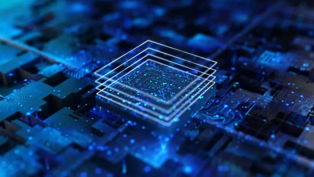
Huawei likens this approach to a long, linear road that is folded over multiple levels to shorten travel distances. In a processor, this logic involves restructuring internal blocks onto more compact layers to reduce transmission delays, enhance density, and optimize performance without solely relying on finer fabrication.
According to Huawei, this strategy operates at multiple levels: components, circuits, chip architecture, and complete systems. The company claims to have already designed and mass-produced 381 chips over the past six years using principles related to this approach.
The Upcoming Kirin 2026 Will Showcase This Technology
The first major product fully utilizing this philosophy is expected to be the upcoming Kirin mobile processor later this year. Huawei indicates that this new architecture will significantly enhance performance, energy efficiency, and logical density.
The company goes even further, asserting that technologies arising from the Tau Law could achieve performance comparable to a 1.4 nm chip by 2031.
However, it’s important to note: this does not necessarily mean Huawei will physically manufacture a true 1.4 nm processor in the traditional sense. Instead, the company advocates that a smarter architecture could yield comparable results without relying solely on the most advanced fabrication processes.
A Technological… and Geopolitical Response
The context is undeniably crucial. Following U.S. restrictions, Huawei has limited access to key technologies in the semiconductor industry, particularly those related to TSMC or ASML.
Thus, the Tau Law also represents a strategic attempt to navigate the constraints imposed by the current geopolitical landscape. Rather than solely competing in the race for nanometer sizes — dominated by a few global players — Huawei seeks to shift competition toward architecture, logical optimization, and signal management.
The Future of Chips May Become More Architectural
Beyond Huawei, this announcement reflects a broader transformation within the industry. As Moore’s Law slows, future gains may come from: 3D stacking, hybrid architectures, AI applied to chip design, or approaches such as logic folding.
Innovation in semiconductors may no longer rely solely on “smaller” but rather on “smarter.” And this is precisely the narrative Huawei aims to promote.