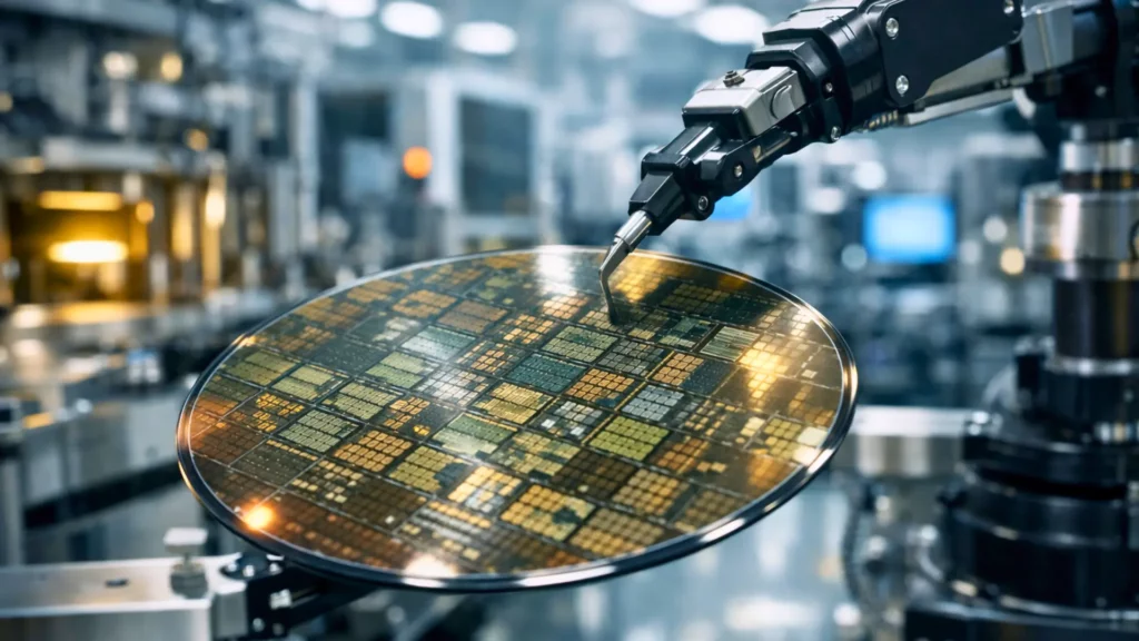
On February 17, 2026, China officially announced the mass production of its first hybrid non-binary electronic chips. This industrial advancement effectively combines binary and probabilistic logic, targeting applications in artificial intelligence, aviation, and intelligent systems, with a clear promise of increased energy efficiency.
Energy and architectural limits of binary logic hinder the evolution of modern processors
Since the dawn of computing, processors have been built around the principles of 0s and 1s. This simple logic underpins all calculations. However, traditional binary logic is now revealing its limitations; it consumes a lot of energy and complicates integration with older systems.
In Beijing, Professor Li Hongge from Beihang University points to a double energy and architectural lock. According to him, current chips generate excessive heat and consume too many resources. Additionally, their rigid design slows adaptation to new uses, prompting the industry to seek a credible alternative.
Probabilistic logic presents a more flexible approach but slows down complex data processing
To overcome these barriers, the Chinese team is exploring probabilistic logic applied to circuits. In this model, the signal is no longer strictly 0 or 1; instead, it depends on a frequency measured over time, allowing for more flexible calculations.
This approach reduces the necessary hardware and decreases power consumption. It is already dominating in advanced image processing and certain neural networks. However, it also increases computation time, leading to a potential reduction in raw performance.
In practice, you gain energy efficiency but lose speed. This constraint thus hampers its widespread adoption. For this reason, engineers are working to find a viable compromise for the industry.
The HSN hybrid system combines binary speed with probabilistic efficiency in a novel architecture
At the heart of this advancement is the Hybrid Stochastic Number system. This architecture merges the two logics to retain the speed of binary while leveraging the energy efficiency of probabilistic logic. With this balance, a new industrial path is opening up.
On the ground, these chips achieve greater fault tolerance and lower power consumption. They also adapt better to intelligent uses. The first models, manufactured using a 110-nanometer process by SMIC, target innovative touch and display chips.
Additionally, in 2023, the team launched a version dedicated to machine learning. Fabricated using a 28-nanometer process, it incorporates in-memory computation algorithms, minimizing data transfers, speeding up processing, and reducing energy consumption.
Active applications and a major strategic issue for the Chinese semiconductor industry
Currently, these chips are deployed in intelligent control systems. In practice, they filter background noise and detect weak signals on touch screens. They achieve microsecond calculation latencies while maintaining software flexibility and stability.
Simultaneously, this breakthrough occurs within a tense geopolitical context. Beijing aims to reduce its technological dependence. Thus, with domestic mass production, China strengthens its position in the semiconductor market and offers a credible alternative to dominant traditional architectures.